Semiconductors
Optical metrology solutions designed for optical testing and qualification needs in lithography manufacturing
Imagine Optic’s Optical metrology for semiconductors and Lithography solutions offer precise optical testing and qualification tools, essential for quality assurance and performance optimization in microchip production and advanced photolithography systems. Using patented metrology systems such as the Parallel Optics Procedure (POP) and leading wavefront sensors, Imagine Optic enables manufacturers to measure and analyze surface shape, transmitted and reflected wavefront errors, and minute aberrations across plane-parallel optics, lenses, and mirrors used in semiconductor fabrication.
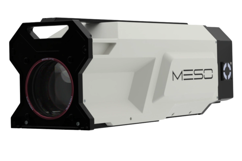
With the MESO metrology instrument and HASO Shack–Hartmann wavefront sensors, users can accurately perform optical testing in reflection and transmission, qualifying each component’s surface figure and overall wavefront error—critical metrics for maintaining high yield and minimizing defects in semiconductor and lithography applications. These real-time measurement systems distinguish subtle defects, track Zernike coefficients to pinpoint specific aberrations, and support both alignment and optimization workflows on production lines and in R&D environments.
Lithography steppers
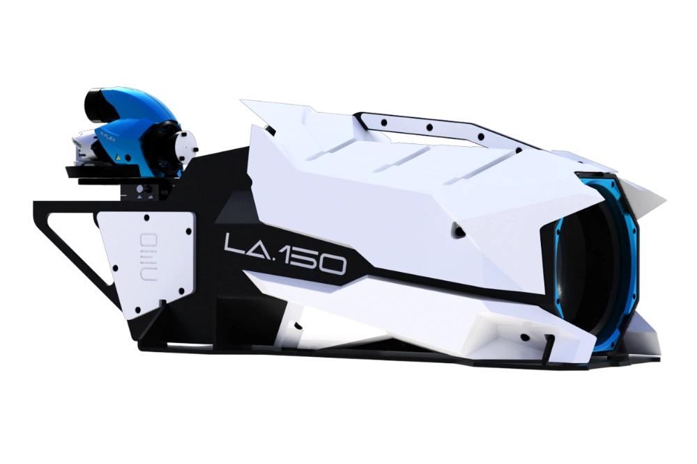
Test the wavefront and pupil quality of projection optics and align complex multi-element optical systems, optics and sources with our Hartmann and Shack-Hartmann wavefront sensors from the EUV and DUV spectral range to the VIS range.

Wafer inspection
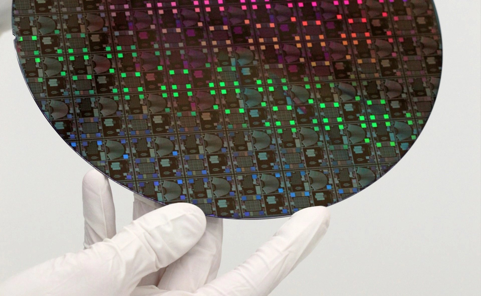
Discover optical metrology instruments developed to test of flat samples and characterize the surface figure and bow of wafers even when vibrations, working distance or wavelength requirements are not compatible with interferometric methods.
UV Laser Testing
For beam testing, collimation, beam pointing adjustment, alignment and aberration control of lasers and complete optical paths up to delivery, choose a compact, easy and quick to set up M2 or wavefront sensing solution combining live phase and intensity measurements.
Implementations - Semiconductors and Lithograpy
|
+ Characterization of projection optics in steppers
|
+ X-ray source generation for semiconductor inspection |
RELATED PRODUCTS – Optical metrology for semiconductors
Copyright 2026 Imagine Optic – All rights reserved
